27.
(Continued)
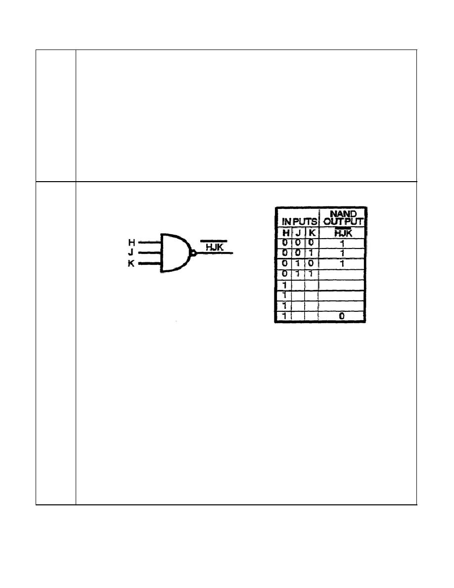
Refer to the NAND-logic diagram on the previous page. The diagram is composed of an AND
gate whose output is NOTted (inverted) by the NOT circuit. The output of the AND gate is the
input to the NOT circuit. The NOT circuit will invert this input and produce the complement at
the output, as shown in the truth table. A NAND gate will ways NOT (invert) an ANDed
expression. Note that the whole quantity of ABC is complemented, not just the separate
variables.
Complete the truth table below for the three-input NAND operation.
IT0342
1-16


 Previous Page
